Maintenance & Technical Guides
Hardware Debugging and PCB Trace Repair: The Low-Level Logic of Hardware Resilience
May
In the broader context of system design, “debugging” is a term usually reserved for the high-level world of software and algorithms. However, for those who seek to master the entire technical ecosystem, debugging must extend into the physical layer. The Printed Circuit Board (PCB) of a mechanical keyboard acts as the “Kernel” of the device—the silent, architectural foundation that routes every electrical signal with absolute precision. When a trace fails or a solder pad is lifted, the entire system suffers a breakdown in immediacy. This article will elucidate the rigorous methods of hardware debugging and PCB trace repair, demonstrating how maintaining the structural integrity of the circuit is a viable and essential skill for any modern technical professional.
1. The PCB as an Architectural Blueprint
To understand hardware failure, one must first appreciate the architectural complexity of the PCB. It is not merely a piece of fiberglass; it is a multi-layered map of copper “traces”—the highways through which electrons travel. Each trace is an integral path that connects a switch to the microcontroller (MCU).
In modern keyboards, these traces are often microscopic. If a trace is severed—whether through a manufacturing defect, a deep scratch during modding, or environmental corrosion—the logic of the circuit is broken. This results in a “Dead Key” or, in the case of a damaged matrix column, an entire row of non-functional keys. Identifying these breaks requires a shift in perspective, moving from a user of the interface to a debugger of the hardware logic.
2. The Debugging Protocol: Signal Continuity and Logic Testing
Just as a software developer uses a debugger to trace the execution of a program, a hardware artisan uses a Multimeter to trace the flow of electricity. This is the first step in establishing a viable repair strategy.
The Continuity Test
The most fundamental tool in hardware debugging is the “Continuity Test.” By placing the multimeter probes at the start and end of a trace, you can determine if the electrical path is complete. If the multimeter fails to beep, the structural integrity of that trace is compromised. This binary feedback allows you to isolate the exact “segment” where the signal fails, providing the immediacy of information needed to proceed with a repair.
Matrix Mapping: Understanding the Grid
Mechanical keyboards use a “Matrix” system (Rows and Columns) to minimize the number of pins required on the MCU. When a failure occurs, the nuance of the symptom often points to the location of the bug.
Single Key Failure: Usually a dead switch or a broken solder joint on a specific pad.
Column/Row Failure: A break in the primary trace that services that entire section of the grid. By mapping the matrix, you can elucidate the underlying logical structure of the board, making the troubleshooting process more efficient.


3. Common Failure Modes: Identifying the “Hardware Bugs”
Before performing a repair, you must diagnose the specific “failure mode” that has disrupted the system’s dominance.
Lifted Pads: This often occurs during aggressive desoldering. The copper pad physically detaches from the PCB, breaking the connection to the trace.
Fractured Traces: Small, hairline cracks in the copper, often caused by the board flexing or by physical impact.
Corrosion (The Silent Killer): In humid environments, moisture can oxidize the copper, slowly eating away at the integral traces until they are no longer conductive.
For a future Solution Architect, recognizing these patterns is the hardware equivalent of identifying common anti-patterns in code. Each requires a specific, logical intervention to restore the system’s viability.
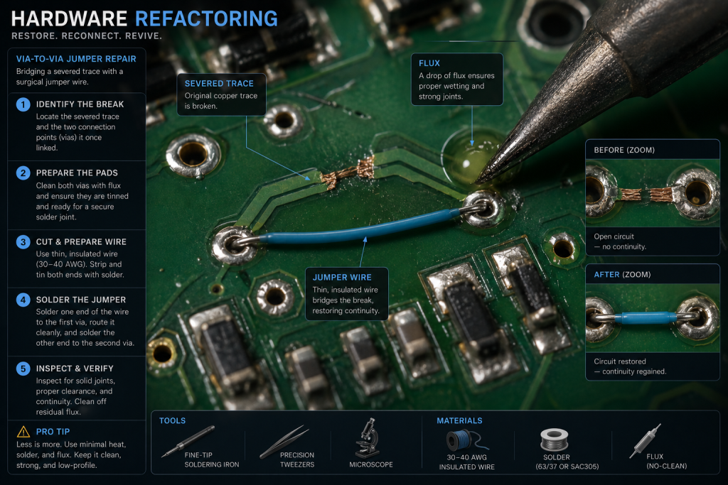
4. The Jumper Wire Protocol: Physical System Refactoring
When a trace is beyond simple repair, the most viable solution is to “refactor” the circuit using a Jumper Wire. This is the process of creating a new physical path for the signal, bypassing the damaged section entirely.
Step 1: Surface Preparation
Using a fiberglass scratch pen or a fine blade, one must gently remove the “Solder Mask” (the green or black protective layer) to reveal the bare copper of the traces or “Vias” (the small holes that connect PCB layers). This requires extreme nuance; apply too much pressure, and you will destroy the remaining copper.
Step 2: The Bridge (Jumpering)
A tiny, insulated copper wire is then soldered from a functional point before the break to a functional point after it. This wire acts as a “Direct Proxy” for the original trace. In software terms, you are “redirecting” a pointer to a new memory address. Once the jumper is in place, the structural integrity of the circuit is restored, and the signal’s immediacy returns.
Step 3: Reinforcement
Because jumper wires are delicate, they must be secured. Using a small drop of UV-curable solder mask or high-strength adhesive ensures that the repair remains viable even under the stress of heavy typing or transportation.
5. Soldering as a Low-Level Language
For someone deeply involved in Software Development, soldering can be viewed as the ultimate “Low-Level Language.” If C or Assembly is the language closest to the CPU, then soldering is the language of the electrons themselves.
The immediacy of a well-executed solder joint—smooth, shiny, and concave—is a sign of technical mastery. A “Cold Solder Joint” (dull and brittle) is a hardware bug that introduces resistance and instability into the ecosystem. Mastering the temperature of the iron and the flow of the flux is integral to creating a system that will last for decades.
6. The Solution Architect’s Mindset: Sustainability vs. Obsolescence
In 2026, the tech industry is moving toward “Right to Repair” and sustainability. From a high-level perspective, the ability to debug and repair hardware is a powerful statement against planned obsolescence.
A viable system is one that can be maintained. By choosing to repair a $200 PCB instead of discarding it, you are demonstrating a commitment to the structural integrity of the entire technical world. This mindset—valuing the longevity of a system and having the technical skill to preserve it—is what separates a true architect from a mere consumer. Whether you are managing a massive cloud architecture or a 60% mechanical keyboard, the principles of resilience and maintenance remain the same.
7. The Synergy of Hardware and Firmware Debugging
A truly sophisticated repair often involves a combination of hardware and firmware intervention. Sometimes, a trace might be so badly damaged that it is impossible to repair physically.
In such cases, a paradigm shift is required: using firmware (like QMK or VIA) to “Remap” the broken key to a different pin on the MCU. This “Software-defined Hardware” approach allows you to maintain the board’s viability even in the face of catastrophic physical failure. It shows the nuance required to balance physical constraints with digital solutions—a core skill for any professional at firms like Google or Facebook.
8. Conclusion: Mastering the Invisible Architecture
Hardware debugging is the process of making the invisible visible. It is the art of seeing the flow of electricity through the architectural layers of the PCB and knowing how to intervene when that flow is interrupted.
To elucidate the true value of this skill: it provides a sense of absolute dominance over your tools. You no longer fear failure because you understand the logic of the repair. By preserving the structural integrity of your keyboard, you ensure that your interface with the digital world remains fast, reliable, and perfectly tuned. As you move toward your internship in September 2026, let your ability to debug both code and hardware be the mark of your versatility and your excellence as a master of systems.